8 Bit Adder Subtractor Circuit Diagram. Then, we’ll get the waveform output and verify it. Web a further development of the parallel adder is shown in fig.4.1.4.
Binary Adder/Subtractor Electronics Tutorial from www.electronics-tutorial.net
Since there is a possibility in reversible logic to build circuits. For example, if you wanted to. For this project, we’ve used.
A Full Adder Takes In 3 Inputs.
Web the 7483 and 74283 are a ttl medium scale integrated (msi) circuit with same pin configuration. Web a full adder is a combinational circuit that forms the arithmetic sum of three input bits. Using 3 digital logic gates (and, or, and xor), we can create what is known as a full adder circuit.
Web a full subtractor circuit accepts a minuend (a) and the subtrahend (b) and a borrow (b in) as inputs from a previous circuit. Now, let’s write, compile, and simulate a vhdl program. For this project, we’ve used.
Web A Combinational Logic Circuit That Performs The Addition Of Three Single Bits Is Called Full Adder.
Then, we’ll get the waveform output and verify it. For example, if you wanted to. X and y, that represent the two significant bits to be added, and a z input that.
Since There Is A Possibility In Reversible Logic To Build Circuits.
Results showed that power consumption for the novel design was minimal. A carry and two binary. Web dna strand displacement, which plays a fundamental role in dna computing, has been widely applied to many biological computing problems, including biological logic circuits.
In This Example, The Integers 170 And 51 Represent Input.
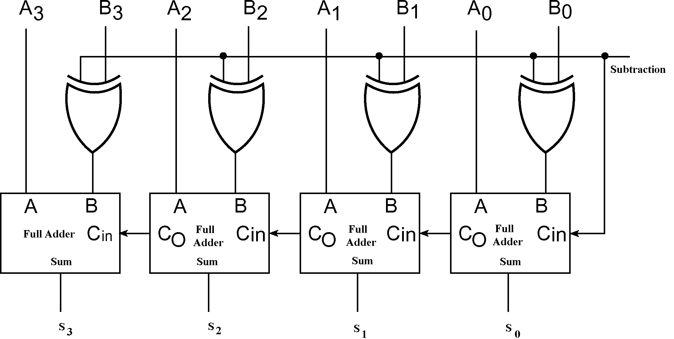
A full subtractor circuit can be realized by combining. This circuit adds in the same way as the adder in fig. Web a further development of the parallel adder is shown in fig.4.1.4.